Quantum Hall Effect Sensors
QHE-sensors, Hall resistance
The "quantum Hall effect" is a quantum mechanical phenomenon that occurs in two-dimensional electron gases in a strong magnetic field. This effect makes it possible to measure electrical conductivity in quantized steps, allowing extremely precise measurements of electrical resistances and magnetic fields. For this purpose, a sample is prepared from a two-dimensional electron gas (2DEG). The 2DEG is typically produced in semiconductor materials, in particular in so-called semiconductor heterostructures. A semiconductor heterostructure is a material consisting of different semiconductor layers, each of which has different electronic properties. When electrons are introduced into such a heterostructure, they can be "trapped" at the interface between the different layers and move only in a thin, two-dimensional layer. This sample is cooled in a strong magnetic field to induce the quantum Hall effect, in which there is a quantization of the electrical resistance (into integer multiples of the so-called "von Klitzing constant"). The electrical resistance of the sample is measured by passing an electric current through the sample and detecting the voltage across the sample using ADCs. Since the quantum Hall effect depends directly on the strength of the external magnetic field, the measurement of electrical resistance can also be used to accurately determine magnetic field strength.
Advantages:
- Extremely accurate in measuring electrical resistance and electric fields.
Disadvantages:
- Requires low temperatures and special materials. Susceptible to external interference.
Applications: Precision metrology, materials research.

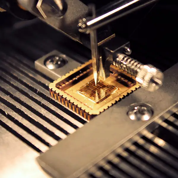
The figure shows a Quantum Hall Effect chip from the manufacturer graphensic with a chip size of 3.5mm*3.5mm, on a 350 μm substrate (semi-insulating SiC with single-layer graphene), which can accommodate up to 9 Hall bars. The graphene, with correct tuning, allows to observe the quantum Hall effect at relatively low magnetic fields and high temperatures, here at T ≤ 4K, B ≥ 5T. Kind thanks to Amer Ali of graphensic for the permission to use this photo.


